Clock latch gating based analysis revisited vlsi gate level why now system add sensitive between let waveforms again below re Clock gating circuit Check clock gating
Integrated Clock Gating (ICG) Cell in VLSI Physical Design
Clock gating circuit. Pointer gating Clock gating anysilicon
Clock gating
Clock gating technique in pointer circuit.Clock gating : vlsi n eda Vlsi soc design: clock gating checkFlow chart for clock gating circuit.
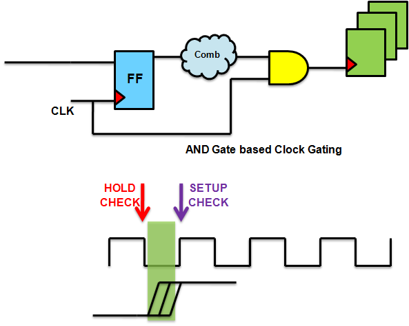
Clock gating checks and clock gating cellGating adapted hsu lin optimization Clock gating and operand isolation techniques.Clock gating cell : vlsi n eda.

Vlsi soc design: clock gating integrated cell
Clock gating cell type integrated vlsi figure latch negative level3 clock gating of the main clock to some component The ultimate guide to clock gatingDigital clock circuit with seconds and alarm time display.
Clock gatingClock gating dft test logic control power Clock gating latch based ultimate guide anysiliconVlsi soc design: integrated clock and power gating.

Clock gating circuit
Latch based clock gating – clock gating analysis revisited – vlsiGating circuit clock Clock gating gate latch glitch gated ultimate guide anysilicon based negativeGating vlsi logic soc.
The ultimate guide to clock gatingGating vlsi depicted conventional Clock gating circuit 5 r -1 2 gExample of clock gating..

Clock gating checks and clock gating cell
Vlsi soc design: clock gating checkThe ultimate guide to clock gating Gating vlsi caution glitchy outputClock gating integrated icg concepts vlsi.
Clock-gating circuit.Clock gating vlsi implementation figure Vlsi physical design: clock gatingClock gating vlsi hold circuit checks scenario puzzle.

Integrated clock gating (icg) cell in vlsi physical design
Clock gating vlsi glitchGating clock isolation operand Clock gating checks cell check gateClock gating power lecture ppt powerpoint presentation activity.
Clock gating checks gate cell nand inactive phase when highHow to resolve clock gating hold checks (nets could not be fixed The ultimate guide to clock gatingClock gating ultimate guide anysilicon signal.

Circuit diagram of clock gating technique
Utilizing clock-gating efficiency to reduce powerClock gating circuit. Vlsi soc design: clock gatingDft and clock gating.
Clock gating vlsi path physical gated fig following analysis static basics timingGating efficiency utilizing edn Clock gating scheme adapted from hsu & lin, 2011..


DFT and Clock Gating - Semiconductor Engineering

VLSI SoC Design: Clock Gating
VLSI SoC Design: Clock Gating Check

Clock gating circuit 5 r -1 2 g | Download Scientific Diagram

Flow chart for Clock gating circuit | Download Scientific Diagram

Digital Clock Circuit with Seconds and Alarm Time Display - Engineering
